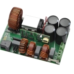
TDTTP4000W065AN Leverages SuperGaNďż˝ FET Performance in Simpler Design
GOLETA, Calif.--(BUSINESS WIRE)--#900V--Transphorm, Inc. (OTCQB: TGAN)�a pioneer in and global supplier of high reliability, high performance gallium nitride (GaN) power conversion products�today announced availability of its newest evaluation board, the TDTTP4000W065AN. Designed for single-phase AC-to-DC power conversion up to 4 kilowatts (kW), this board uses the bridgeless totem-pole power factor correction (PFC) topology with a traditional analog control. This pairing provides fast and easy access to the top-notch conversion efficiency made possible by Transphorm�s latest SuperGaN� FETs without the need for firmware development required when using digital signal controllers (DSCs).
Driving GaN Adoption with RDDR
Transphorm�s innovation path for its high voltage GaN platform and related design tools centers on delivering best-in-class GaN Reliability, ease of Designability, ease of Drivability and high-volume Reproducibility (RDDR). To that end, the TDTTP4000W065AN offers power systems engineers an upgrade in efficiency over standard CCM Boost PFC designs that use superjunction MOSFETs.
The evaluation kit is rated at 4 kW highline (180-260 V) and 2 kW lowline (90-120 V). The main advantages of the analog totem-pole solution follow:
- Maintenance power�power required to support basic functionality such as powering up and supplying chipsets�is a relatively fixed amount in any system. Therefore, as an application�s power level decreases, the maintenance power becomes a larger percentage of the system�s overall power loss. When compared to a DSP solution, Transphorm�s analog board requires lower maintenance power at the onset, thereby increasing overall system efficiency.
- No DSP firmware programming is needed, suitable for standard CCM boost AC-to-DC PFC power stages.
For engineers requiring more design flexibility, Transphorm released the TDTTP4000W066C earlier this year. This DSC-based 4 kW AC-to-DC board also uses the bridgeless totem-pole PFC with the company�s SuperGaN FETs. However, it integrates a dsPIC33CK DSC board from Microchip that has been preprogrammed and is backed by dedicated firmware support.
�Transphorm�s analog evaluation board provides an unprecedented opportunity to access our highly efficient GaN in the easiest way possible. Much like the preceding digital board, it gives power system engineers a choice that the high voltage device market was previously lacking,� said Philip Zuk, VP of Worldwide Technical Marketing and NA Sales, Transphorm. �Regardless of the end application�s targeted value proposition, we have the diverse toolset and the most robust GaN possible to help you succeed.�
SuperGaN Devices: Performance Beyond Superjunction MOSFETs
The TDTTP4000W065AN employs Transphorm�s SuperGaN Gen IV TP65H035G4WS FETs in the board as the fast-switching leg with low-resistance Silicon MOSFETs in the slow-switching leg. The resulting performance is similar to that of its digitally controlled counterpart, the TDTTP4000W066C.
The TP65H035G4WS is a 650-volt device with a 35 milliohm on-resistance in a TO-247 through-hole package with an inherently high thermal dissipation ability. This feature eliminates the need to parallel devices for higher power output, a design method required by competitive surface-mount GaN solutions. And, as with all other Transphorm GaN devices, the SuperGaN FETs can be driven with a threshold voltage (Vth) of 4 volts and standard off-the-shelf gate driver operating from 0 to 12 volts.
Availability
The TDTTP4000W065AN evaluation board is currently available through Digi-Key and Mouser.
About Transphorm
Transphorm, Inc., a global leader in the GaN revolution, designs and manufactures high performance and high reliability GaN semiconductors for high voltage power conversion applications. Having one of the largest Power GaN IP portfolios of more than 1,000 owned or licensed patents, Transphorm produces the industry�s first JEDEC and AEC-Q101 qualified high voltage GaN semiconductor devices. The Company�s vertically integrated device business model allows for innovation at every development stage: design, fabrication, device, and application support. Transphorm�s innovations are moving power electronics beyond the limitations of silicon to achieve over 99% efficiency, 40% more power density and 20% lower system cost. Transphorm is headquartered in Goleta, California and has manufacturing operations in Goleta and Aizu, Japan. For more information, please visit www.transphormusa.com. Follow us on Twitter @transphormusa.
Contacts
Heather Ailara
211 Communications
P: +1.973.567.6040
[email protected]


